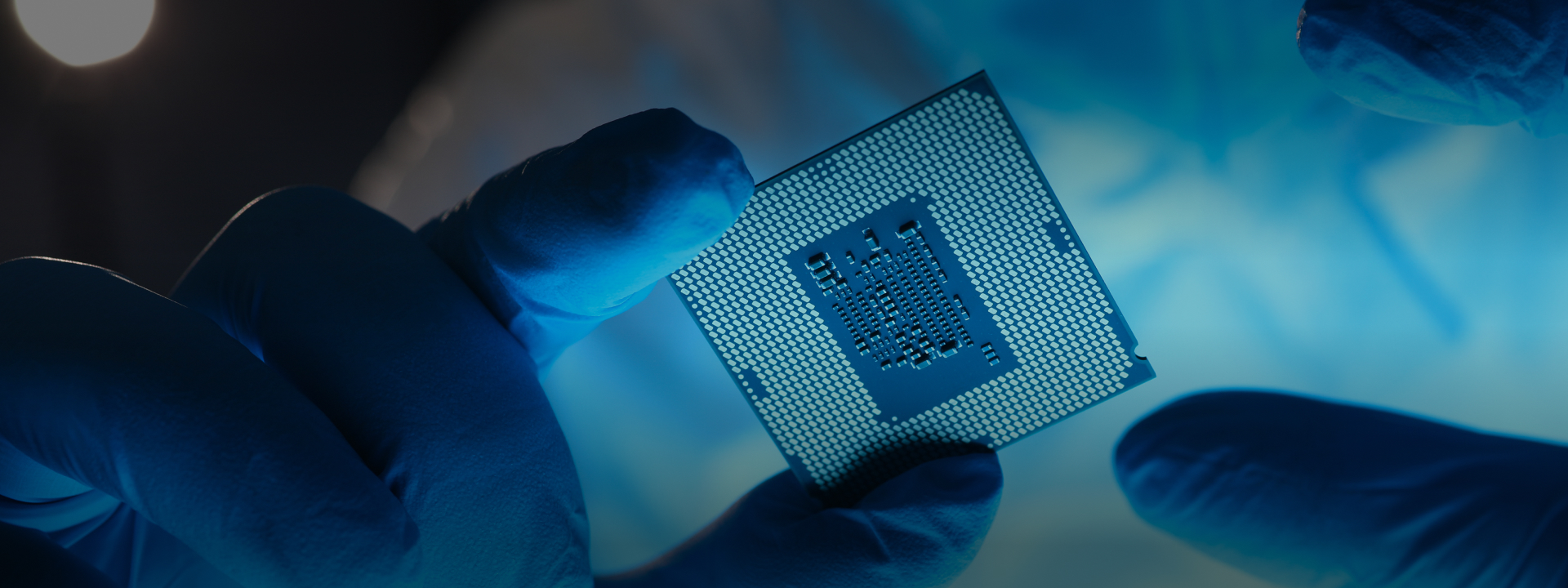
LB Lusem's BGBM (Back Grinding Back Metal) technology is applied to power devices in all electronic circuits where batteries are used, such as Smartphone, Navigation, TV, Audio, Server power, etc., where MOSFET (Metal-Oxide Semiconductor Field Effect Transistor) products are used. /It is the technology that can be applied.
In order to realize customer satisfaction, the company has developed a turn-key business based on differentiated technology from the existing commercialized MOSFET PKG process. Realization is the vision of the business.
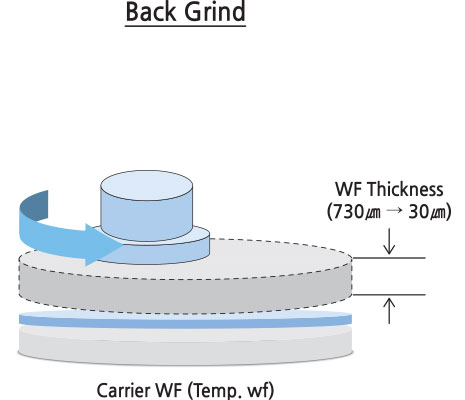
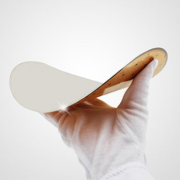
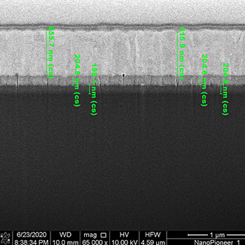
We have the best technology through re-establishment of process flow, and by securing wafer level 30~50um Full Grind technology, we realized low resistance and low heat conduction by reducing wafer thickness.
BSM (Back Side Metal), which is responding to the level of 30um, is also prepared to be modified and supplemented according to customer requests.
The power device of the electronic device battery applied with the company's superior technology increases the life time by reducing standby power, and provides a solution for customer satisfaction with the best product through a thorough inspection process.
In order to go one step further as a Best Partner, we are doing our best to continuously develop products based on the best products and L/T (Lead Time) reduction through Process Optimize.
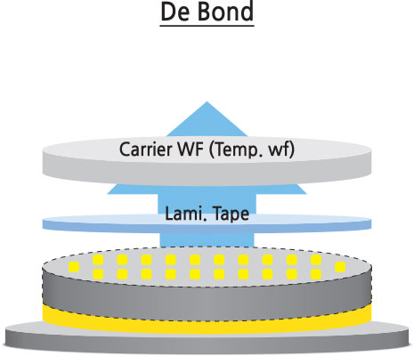
 Back Grinding
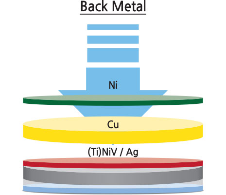
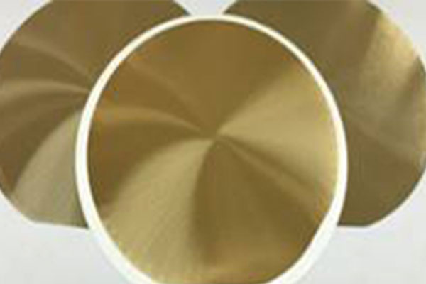 Back Side Metal
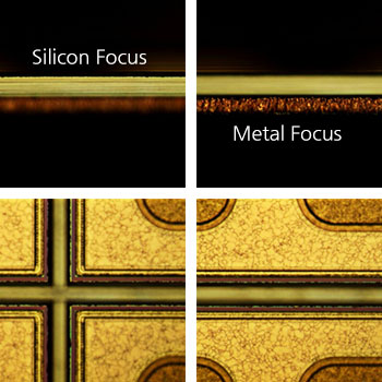
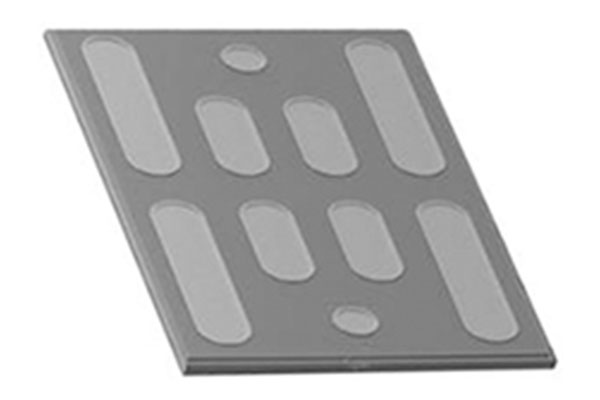 MOSFET Top View
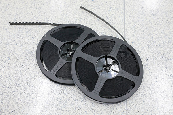 Tape&Reel
-
[ Spec & Target ]
- Wafer Thickness (8 inch) : 30 ~ 100 um
- Sputter Target : NiV/Ag (Opt. Ti AV)
-
- Wafer Thinning Technology
- Silicon Thickness Target : Min 30um
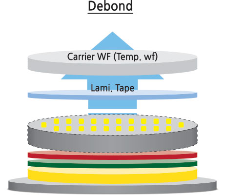
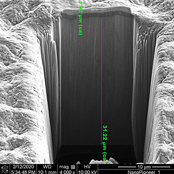
- Full Grinding through TBDB Method
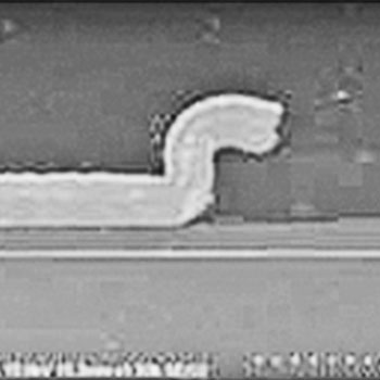
- Cost Reduction through increasing Net die(about 7%)
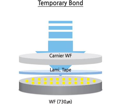
- Wafer Crack Free through TBDB Method
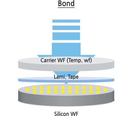
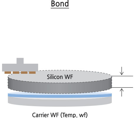
- Wafer Warpage Free through Carrier Wafer Bonding
-
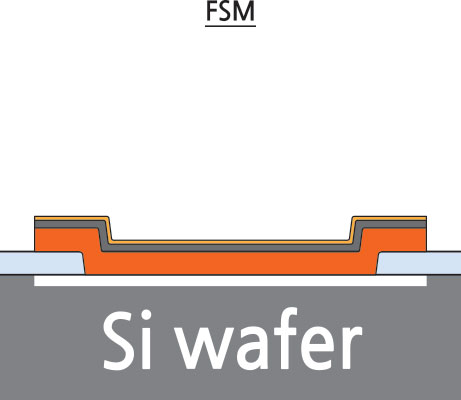
- Offering FSM(Front Side Metal) Servic
- CNA Bumping available
- ENIG / ENEPIG(Under develop)
- Full Tern-Key Solution including FSM
-
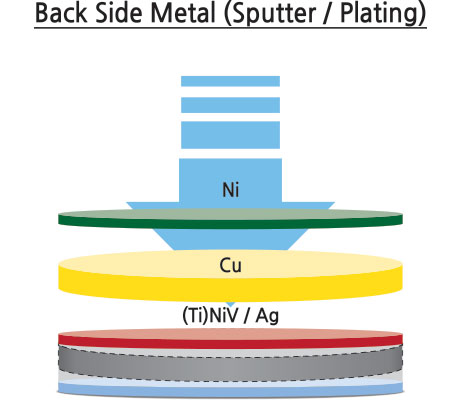
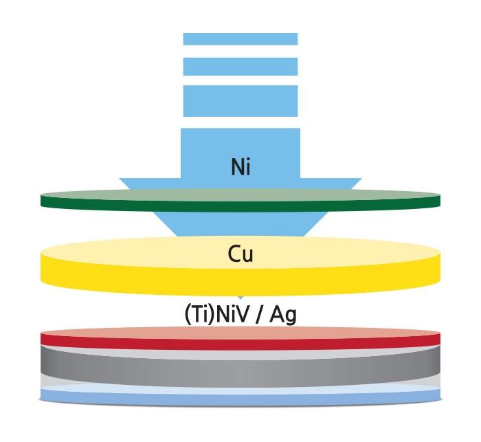
- Various Sputtering deposition available
- Ti / NiV / Ag
- NiV / Ag
- Ti / Cu
-
- Optimized BSM Thickness condition
- Cu/Ni
- Cu Thick target 50um for thin wafer
- Low Rsson characteristic for Mosfet
-
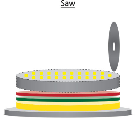
- Clear Cut Lin
- Blade Sawing
- Laser Sawing
-
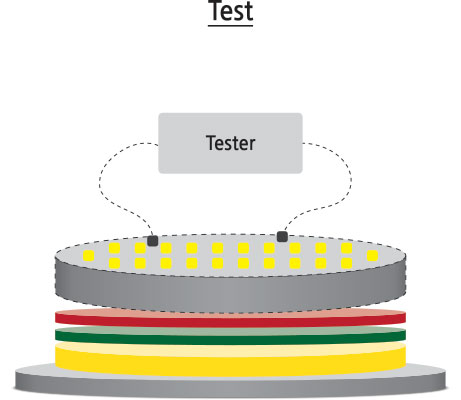
- Test & Tape and Reel
- Probe Test available(ETS200)
- Tape and Reel packing available
- Offering Full Turn-Key Solution
- Turn-Key Solution -> Reducing Lead Time
- Customized Mass Production -> Meeting Customer needs