
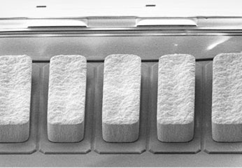
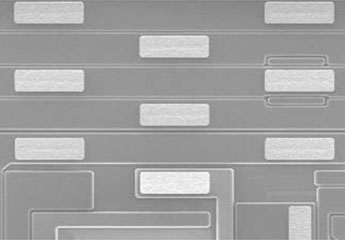
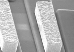
BUMP
Bumping refers to a process of forming an external connection terminal (bump) having a size of 5 to 20 μm on a wafer AI pad such as Au or a solder. Bumps on Die surface can perform various functions. Providing electrical connection to the substrate, and heat transfer from the chip to the substrate to prevent heat dissipation, shorting, and physically supporting the chip.
Produce Specification
| Produce Specification | |
|---|---|
| Item | Capability |
| Wafer | 8 inch |
| Hardness | Middle Level : 60±20um High Level : 90±20um |
| Bump Height (Typical) | 8 ~ 14um |
| Height Uniformity | WID : ≤2um WIW : ±2um |
| Bump Pitch | Straight 21um, Staggered 13um |
| AOI | 2D |
Process Introduction